
TL;DR · 30-second read
The Short Version
The world’s two largest advanced chip factories, Taiwan Semiconductor Manufacturing Company and Samsung, have agreed to buy the newest chip-printing machines from the Dutch equipment maker ASML. These machines use light to print circuit patterns onto silicon wafers, a bit like a photographic enlarger working at a scale smaller than a virus.
ASML and the Taiwanese chipmaker also plan to switch to glass stencils twice as wide as today’s. Wider stencils mean bigger chips can be printed in one shot, and bigger chips printed in one shot are cheaper chips. Those are the chips that run artificial intelligence.
ASML has secured commitments from Taiwan Semiconductor Manufacturing Company (TSMC) and Samsung Electronics for its newest generation of extreme ultraviolet (EUV) lithography systems, according to Bloomberg, with CNBC and Seeking Alpha reporting the same commitments and tying the demand to the artificial-intelligence buildout. Separately, Focus Taiwan and EU Today reported that TSMC and ASML are working together on 12-inch EUV photomasks, a step up from the 6-inch masks that have been the industry standard for decades, intended to widen what High-NA machines can print.
Neither the tool commitments nor the photomask programme came with disclosed unit volumes, pricing, delivery dates or the process nodes involved. What is established is the direction: the two largest advanced-logic manufacturers on the planet have now publicly aligned themselves with ASML’s next lithography platform, and one of them is prepared to change the format of the mask itself to get more out of it.
Executive Summary
Lithography is the step in chipmaking where a circuit pattern is projected onto a silicon wafer. ASML is the only company in the world that builds EUV lithography systems, and its High-NA generation — ‘NA’ meaning numerical aperture, a measure of how much light the lens can collect and therefore how fine a pattern it can resolve — is the successor platform that the entire logic roadmap eventually has to migrate to. TSMC and Samsung committing to those tools removes the largest open question about High-NA: whether the volume foundries would adopt it, or ride existing EUV with multiple patterning for another generation.
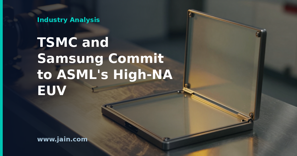
The photomask news is the more technically interesting half. A photomask is the stencil carrying the circuit pattern; today it is a 6-inch quartz plate, and its size sets a hard ceiling on how large a single chip can be. High-NA optics buy resolution by narrowing the printed field, which makes that ceiling lower, not higher — precisely the wrong direction for AI accelerators, which are among the largest chips ever manufactured. A 12-inch mask is the industry’s way of buying the field back.
For anyone buying AI compute rather than making it, the through-line is cost per die. If large accelerators can be printed in one exposure on a next-generation tool instead of being stitched together or broken into smaller chiplets, the economics of every downstream layer — server, rack, data centre, inference price — shift in the buyer’s favour, eventually.
The Mask, Not the Machine, Is the Constraint
Standard lithography prints an exposure field of roughly 26 by 33 millimetres, and the size of a single chip cannot exceed it. That is the ‘reticle limit’, and the largest AI accelerators and their high-bandwidth memory stacks have been pressed against it for years. High-NA EUV improves resolution using anamorphic optics that magnify differently in each direction, and the price of that trick is a printed field roughly half the conventional size. A foundry adopting High-NA for critical layers therefore inherits a smaller canvas at exactly the moment its most valuable customers want a larger one.
Moving the mask from 6 inches to 12 inches attacks that directly: a bigger stencil is what allows a bigger field to be projected in a single exposure. The engineering consequences ripple outward — mask blanks, pellicles, writing tools, inspection and repair equipment, scanner stages and reticle handling all assume the incumbent format. That is why a joint TSMC-ASML effort matters more than a unilateral one. Mask formats are effectively an industry standard, and standards move when the largest buyer and the sole tool supplier move together.
AI Accelerator Economics Are Driving the Roadmap
Historically, lithography generations were pulled forward by mobile and PC volumes, where the metric that mattered was transistors per dollar across hundreds of millions of small dies. The demand now being cited for these tools comes from a different shape of customer: relatively low unit volumes of extremely large, extremely expensive dies sold into data centres. For that customer, yield loss on a big die is brutal — defects scale with area — and every millimetre of printable field is margin.
This is also a reminder of where the bottleneck in the AI buildout actually sits. Public attention fixes on power and cooling, and those are real constraints. But the supply of leading-edge accelerators is gated upstream by a single Dutch tool vendor’s output and by the willingness of two or three foundries to commit capital years ahead of revenue. TSMC’s capital cadence remains visible in its filings — in a 6-K filed with the SEC on September 1, the company adjusted its first-quarter 2026 cash dividend to NT$7.00000137 per common share, payable October 8, following a board-approved distribution of NT$181.5 billion — a reminder that this capital intensity coexists with substantial cash returns to shareholders.
Who Gains, and What Has to Go Right
ASML is the clearest beneficiary. It has no competitor in EUV, and commitments from both leading foundries convert High-NA from a technology bet into a platform with a customer base. TSMC gains optionality: it can keep extending existing EUV with multiple patterning where that is cheaper, and deploy High-NA where the layer count justifies it, while shaping the mask format that its own largest customers will design against. Samsung’s commitment is competitively significant on different terms — foundry share is won partly on the credibility of the next node, and being absent from the next lithography platform would have been a liability.
The risks are not trivial. Larger masks mean larger, heavier, more expensive reticles moving through a machine whose overlay budget is measured in fractions of a nanometre; a 12-inch blank supply chain has to be built and qualified; and the mask ecosystem’s inspection and repair tooling has to follow. There is also a live alternative. The industry’s current answer to the reticle limit is disaggregation — splitting a large chip into chiplets and reassembling them in advanced packaging. If packaging keeps improving quickly, some of the value of a bigger field is captured elsewhere. The likeliest outcome is that both paths advance together, with larger single-exposure dies making the packaged modules themselves more capable.
Background
ASML, based in Veldhoven in the Netherlands, is the world’s only manufacturer of extreme ultraviolet lithography systems, the machines that print the finest features on leading-edge chips. Its equipment is therefore a chokepoint for the entire advanced semiconductor industry, and a recurring subject of export-control policy. TSMC is the largest contract chipmaker in the world, manufacturing processors designed by others, including most of the leading AI accelerators. Samsung Electronics runs both its own memory and logic products and a foundry business competing with TSMC for external customers.
The photomask format at issue has been stable for decades: 6-inch square plates, with a standard exposure field that fixes the maximum size of any single chip. That constraint was largely academic when the industry’s economics were driven by small mobile and PC processors. It became a first-order commercial problem once AI accelerators, built as the largest practical dies and surrounded by stacked memory, became the most profitable products in the industry. Source: ASML and TSMC plan larger masks to expand High-NA chipmaking — report that ASML and TSMC intend to adopt 12-inch photomasks to widen the printable field of High-NA EUV systems. Primary sources: Taiwan Semiconductor Manufacturing Company, Form 6-K filed September 1, 2026 (adjustment to cash dividend per share); ASML Wins Over Top Chipmakers for New EUV Machines — Bloomberg; TSMC, Samsung commit to ASML’s newest chipmaking tools as AI drives demand — CNBC; TSMC, ASML partner on 12-inch EUV photomasks for advanced chips — Focus Taiwan; ASML wins commitments from Samsung, TSMC for new chipmaking gear — Seeking Alpha; ASML and TSMC plan bigger masks that could lower chipmaking costs — Stock Titan.Sources