
TL;DR · 30-second read
The Short Version
Two major chipmakers, GlobalFoundries and Taiwan Semiconductor Manufacturing Company, the world’s largest contract chipmaker, have struck a $2 billion deal to make a key chip part in the United States.
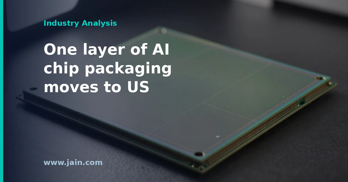
The part is a silicon “interposer”: a thin slab of silicon that sits under an artificial intelligence processor and wires it to its memory, like a shared floor both chips are mounted on. The packaging step built around it has been one of the main limits on how many artificial intelligence chips get shipped.
Making it in America could add supply outside Taiwan. But it covers one step, not the whole chip.
Yahoo Finance reported that GlobalFoundries and TSMC have reached a $2 billion deal for silicon interposers produced in the United States. Silicon interposers are the base layer in the advanced packages that join high-end AI processors to stacked high-bandwidth memory, which places the agreement inside the part of the GPU supply chain that has repeatedly constrained output.
The deal follows TSMC’s October 8 Form 6-K, its September 2026 revenue report, which showed consolidated revenue of roughly NT$511.86 billion for the month, up 54.6 percent from September 2025, and NT$3,898.73 billion for January through September, up 41.1 percent year over year.
Executive Summary
The headline facts are simple: a $2 billion agreement between the world’s largest contract chipmaker and a US-headquartered specialty foundry, covering a component that is made in the United States. The interposer is not a commodity part. It is a large piece of silicon, patterned in a wafer fab with fine wiring and vertical connections called through-silicon vias. AI accelerators mount their compute die and memory stacks on it side by side.
That matters because AI chip supply has been gated less by the ability to make processors than by the ability to package them with memory. Making interposers in the US adds a domestic source for one input to that packaging flow. However, an interposer is an intermediate part. Until the companies say where the rest of the package is assembled, the deal shows where part of the bottleneck can be relieved, not that it has been.
For GlobalFoundries, a $2 billion commitment tied to AI packaging is a significant new line for a foundry that stepped back from the leading-edge process race in 2018. For TSMC, whose September revenue alone was more than NT$500 billion, the deal is small in financial terms. Its importance is geographic and logistical.
Why the Interposer Sits on AI’s Critical Path
The most capable AI accelerators are not a single chip. They are assemblies. A large processor die sits next to several stacks of high-bandwidth memory (HBM), DRAM chips stacked vertically to deliver very fast data access. These parts have to talk to each other across thousands of extremely fine connections, far denser than an ordinary circuit board can carry. The silicon interposer solves this. It is a slab of silicon wired with lithography, the same patterning process used to make chips, so the processor and memory can be packed millimetres apart and connected at chip-level density.
TSMC’s version of this approach is CoWoS, short for chip-on-wafer-on-substrate. Dies are bonded onto an interposer wafer, which is then mounted on a conventional package substrate. In recent years, CoWoS capacity has been widely identified as a binding constraint on AI accelerator shipments. The processors could be fabricated, but there was not enough capacity to package them with their memory. Interposers are one input to that flow. Because they are made in a fab rather than an assembly house, adding interposer supply requires wafer capacity with the right tooling, not just more packaging lines.
What Onshoring One Layer Does, and What It Doesn’t
This is the substance behind the headline. A US-based interposer source moves one fab-made step of AI packaging onto American soil. That has real value. It adds a source outside Taiwan for a component tied to a known chokepoint. It suits a mature, non-leading-edge process, which plays to GlobalFoundries’ strengths in its New York and Vermont fabs. It also gives chip designers and their hyperscale customers, the largest cloud and AI operators, a domestic option to cite when they are asked about supply resilience.
But an interposer alone does not make a finished accelerator. After the interposer is made, the processor dies and memory stacks must be bonded onto it. The assembly must then be mounted on a substrate, tested, and shipped. If those steps remain in Taiwan, US-made interposers simply cross the Pacific in the opposite direction from the processors. Much of the processor output from TSMC’s Arizona fabs has itself needed to return to Taiwan for advanced packaging. The deal becomes a genuinely domestic AI supply chain only when it pairs with US assembly capacity. TSMC said in March 2025 that its expanded Arizona plans include advanced packaging facilities, and its October 6-K shows continued financial support for US subsidiaries, recording lending to TSMC Washington and guarantees for TSMC Arizona. Connecting the interposer supply to that assembly capacity is the step that would turn a single onshored layer into an onshored package.
The packaging variant also matters. TSMC’s family includes the original CoWoS-S, which uses a full silicon interposer, and newer variants such as CoWoS-L, which replace the full interposer with smaller embedded silicon bridges. If flagship accelerators continue shifting toward bridge-based designs, the market for full-size interposers looks different. Which products these US interposers serve will determine how much of the bottleneck they actually touch.
Reading $2 Billion Against Each Company’s Scale
For TSMC, the figure is modest. Its September revenue was about NT$511.86 billion, and its year-to-date revenue was NT$3,898.73 billion, up 41.1 percent. A $2 billion agreement is not a material financial event at that scale. It is a capacity and location decision. Choosing a domestic partner for a mature-process component frees TSMC to focus its own capital elsewhere while adding a US element to its packaging chain.
For GlobalFoundries, the calculus runs the other way. A foundry that chose in 2018 to stop pursuing the most advanced process nodes now has a direct line into the most supply-constrained segment of the AI hardware market, using processes it already runs. That makes it a significant win, though its annual revenue impact cannot be assessed until the contract’s duration and ramp are known. The two companies were once adversaries in a patent dispute that they settled in 2019 with a broad cross-license. A supply relationship on AI packaging is a notable evolution from that history.
Background
TSMC, founded in Taiwan in 1987, is the world’s largest contract chipmaker. It manufactures processors for most leading AI chip designers, and its CoWoS packaging has become central to AI accelerator supply. It is building fabs in Arizona and has said its US plans include advanced packaging. GlobalFoundries, spun out of AMD in 2009, runs fabs in Malta, New York; Essex Junction, Vermont; Dresden; and Singapore. It stopped pursuing the most advanced process nodes in 2018 to focus on specialty technologies.
The two companies settled a patent dispute in 2019 with a broad cross-license. Their new interposer agreement places GlobalFoundries’ US mature-process capacity inside the AI packaging flow that TSMC dominates. Source: GlobalFoundries and TSMC reach $2B deal for US-based silicon interposers (Yahoo Finance): report of a $2 billion agreement covering US-made silicon interposers. Primary sources: Taiwan Semiconductor Manufacturing Company, Form 6-K filed 2026-10-08 (TSMC September 2026 Revenue Report).Sources